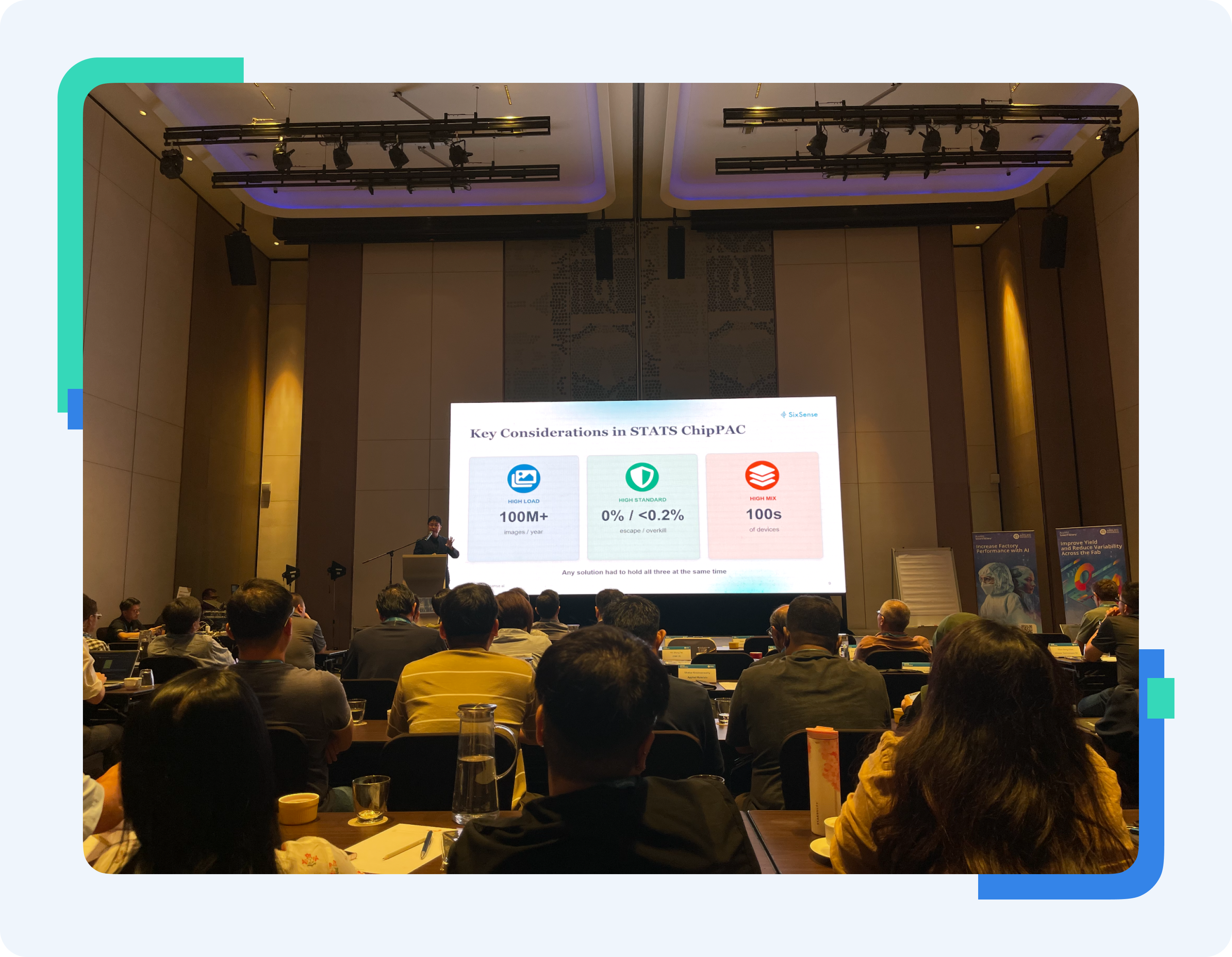
July was a big month at SixSense. We welcomed two new customers—one a global IDM and the other one of the world's largest OSATs, expanding our footprint across both front-end manufacturing and packaging. We also presented our production deployment with STATS ChipPAC at the Applied Materials Symposium in Penang, sharing real-world results from one of the industry's largest OSATs. And we published a new case study from a leading foundry, highlighting how AI has been running in live SEM inspection for nearly two years with high automation, near-zero escapes, and minimal retraining. Here's a look at what happened.
Global IDM Selects SixSense for AI-Powered AOI
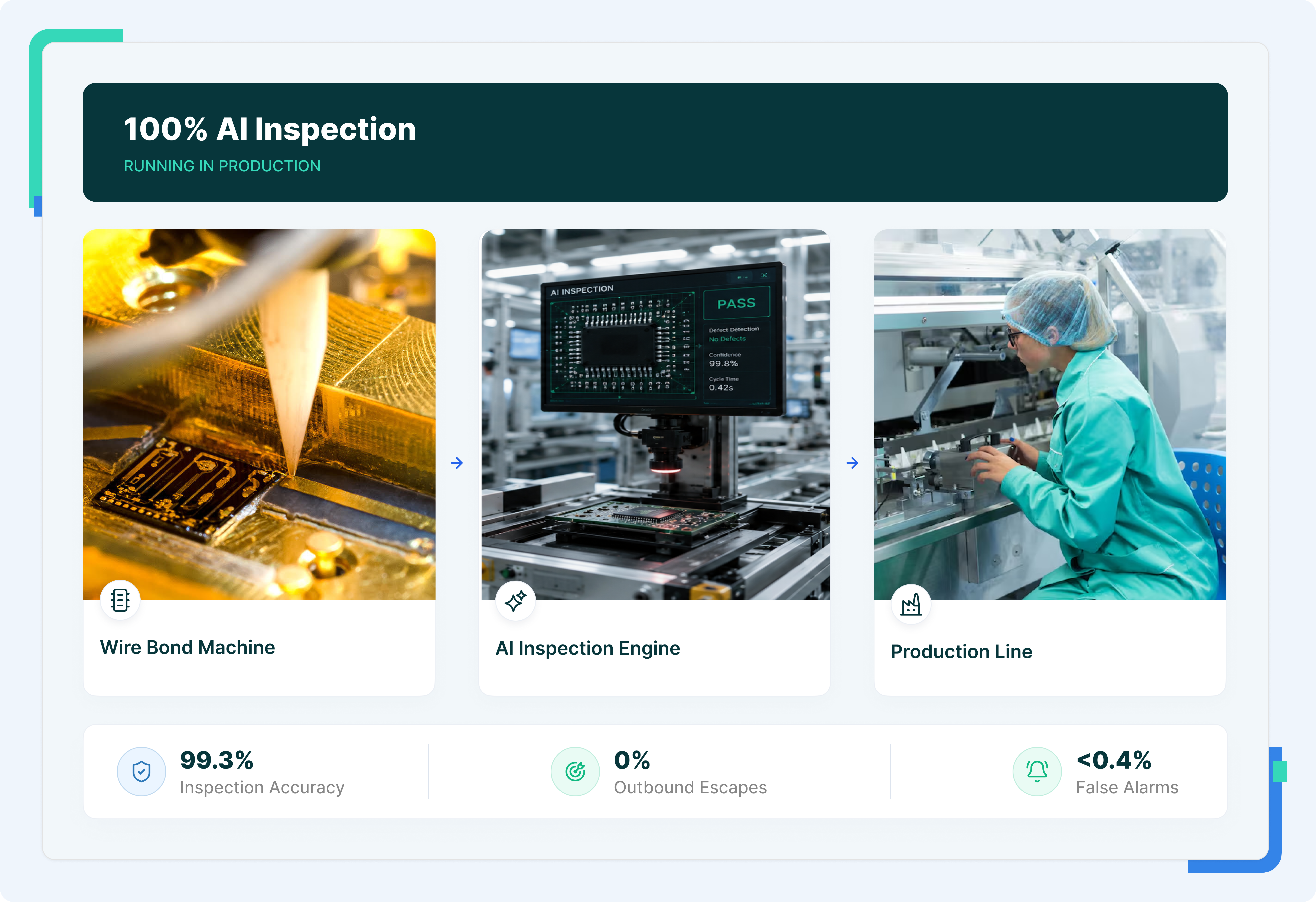
This month, we signed a global IDM to deploy SixSense AI-ADC inside a vision partner's AOI equipment for post wire bond inspection. AI now checks 100% of the images on the line, in real time, without AOI classifying them as good or reject, becoming the primary inspection engine for the production line.
The goal was to remove the AOI recipe problem. Rule-based AOI needs hundreds of device-specific recipes. Each one has to be manually created, tuned and continuously maintained as the products change. That is slow and costly to scale across 1000s of devices. With SixSense , a single AI model replaces 100s of them, dramatically reducing engineering effort. This is a real shift in AOI. Fabs are moving away from rule-based systems that are hard to set up and keep running. They are choosing AI-first inspection that is simpler to manage.
The production deployment delivered >99.3% accuracy, 0% escapes and <0.4% over-rejection. Even defect classes with fewer than 20 training images reached production-grade performance using SixSense's pretrained semiconductor foundation model. More broadly, this reflects a trend we're seeing across the industry: manufacturers are beginning to replace rule-based inspection with AI-first inspection systems that are simpler to deploy, easier to maintain and better suited for increasingly complex semiconductor manufacturing.
One of the World's Largest OSATs Signs SixSense
July also marked another important customer win as one of the world's largest OSATs selected SixSense. The main goal for the customer was to standardise how AI is developed, launched and maintained across the factory. The engineers needed a single platform to prepare data, train models, validate performance, monitor production accuracy and continuously improve AI as new products and defect patterns emerge. They also wanted to reduce repetitive engineering work and make it easier to adopt the latest AI technologies without disrupting production.
SixSense brings all of these workflows together in one no-code platform designed for manufacturing engineers. The result is faster model releases, higher engineering productivity and a continuous feedback loop that keeps production AI improving over time. As AI adoption accelerates, we're seeing customers invest not only in better AI models, but also in the infrastructure required to manage hundreds of production AI models over many years.
SEM Review at a Leading Foundry: 90% Automated for 2 Years
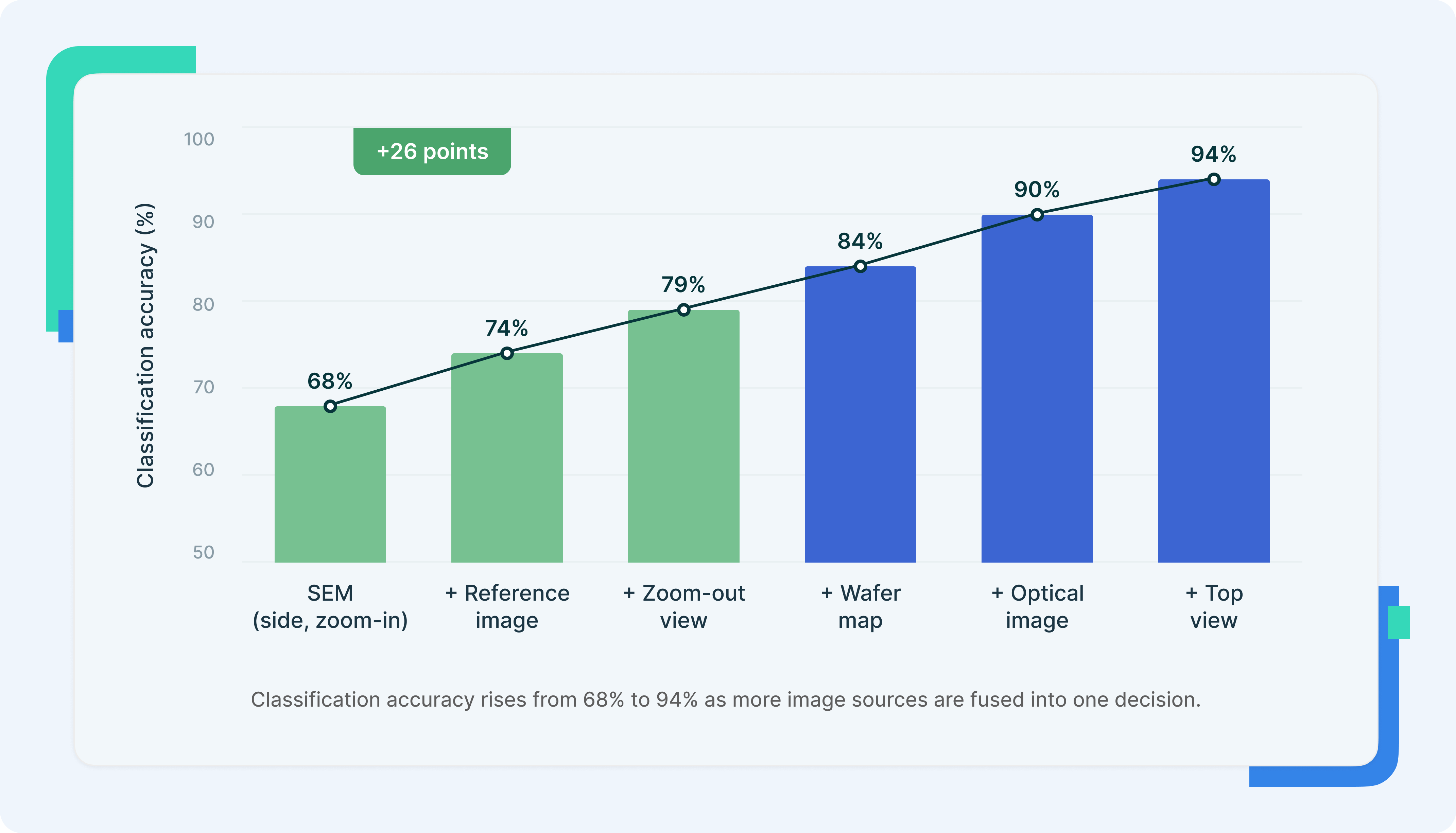
This month we also published a new case study from one of the world's leading logic foundries. Before SixSense, more than 20 operators manually reviewed SEM defect images. Classification accuracy remained below 75%, creating a bottleneck for wafer disposition and slowing responses to process excursions.
Today, SixSense automates more than 90% of SEM images, improves classification accuracy to above 90%, reduces false alarms and helps engineers respond faster to yield issues. Much of that improvement comes from combining multiple SEM views, optical images, wafer maps and reference images into a single AI decision, rather than relying on a single inspection image.
The milestone we're most proud of, however, came long after deployment. Every model launched at the beginning of the program is still running today. Nearly two years later, the system continues to maintain around 90% automation and over 90% accuracy with almost no retraining. For us, that's the real benchmark of production AI; not simply working on day one, but continuing to deliver value year after year.
Advanced Packaging Takes Centre Stage in Penang
We presented our full STATS ChipPAC deployment on stage at the Applied Materials Symposium in Penang. We walked through the whole story of what the fab looked like before AI, their first try with OEM ADC, why they chose SixSense and where the line is today. The biggest accomplishment for this fab is zero escapes at over 99.7% yield. It does this on fewer than 20 AI recipes across hundreds of devices, where most fabs need over 100 models.
Advanced packaging was the topic everyone wanted to talk about. As chips get smaller and packaging gets denser, defect rules get much tighter. That makes AI-ADC in packaging even more useful.
The symposium also highlighted Malaysia's growing semiconductor ecosystem. InvestPenang's CEO opened the event by speaking about the country's growing need for engineering talent and how every engineering job creates several more across the supporting ecosystem. Throughout the day, we had valuable conversations with foundries, OSATs, IDMs and equipment makers from across the region. It was exciting to see how strongly AI for semiconductor manufacturing continues to resonate.