

OEM AOI tools are tuned for high recall, which means they ship with a large fraction of false positives. A second classification layer is standard practice to clean this up. Its role is to reject the false positives and correctly bin the true positives coming out of AOI to enable RCA. But even at this 2nd classification layer, some genuine defects are difficult for AI to spot by looking at the flagged die image only. The defects only become identifiable when the flagged die is compared against a known-good adjacent die: the same die-to-die comparison principle the OEM tool uses. Without that comparison, these defects could escape.
This creates a challenge:
- If we skip comparison with a good die at the 2nd AI classification layer → there is a risk of escape
- However, by using conventional die-to-die matching → we could reintroduce the bulk of false positives that made OEM over reject in the first place, defeating the purpose of having a 2nd AI layer.
The core challenge: How do we pull die-to-die comparison into the 2nd classification layer to prevent escapes, without recreating OEM-level overkill?
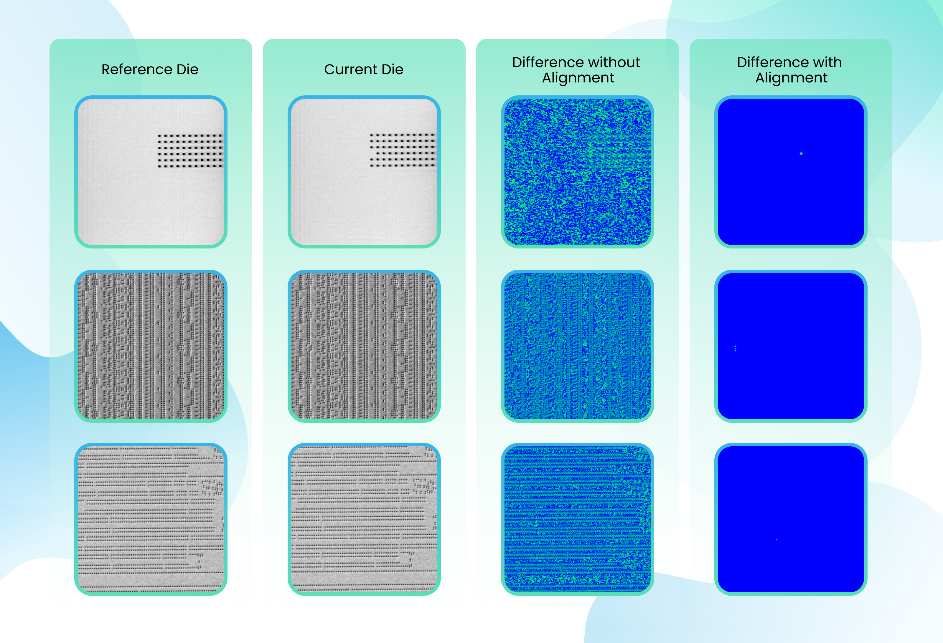
What we found is that a major driver of these false positives is something surprisingly simple: mild image shifts between the reference and test die image. Even a fraction of a pixel of misalignment causes every edge in the image to register as a "difference," flooding the pipeline with nuisance defects.
This article describes a translation-based relalignment technique that resolves this specific failure mode. By aligning die images to sub-pixel accuracy in ~5 ms per pair (down from ~300 ms), the method:
- Prevents escapes by ensuring real defects are not buried under alignment noise.
- Avoids overkill due to high sensitivity
- Runs fast enough to be deployed even directly at the OEM level with no added throughput overhead making it a practical technology to be used at the 2nd AI inspection layer and even at the first detection layer inside OEM workflow.
The remainder of the article walks through why alignment matters, how we approach this problem and the measured impact of such an approach.
1. AOI, False Positives, and a 2nd Classification Layer
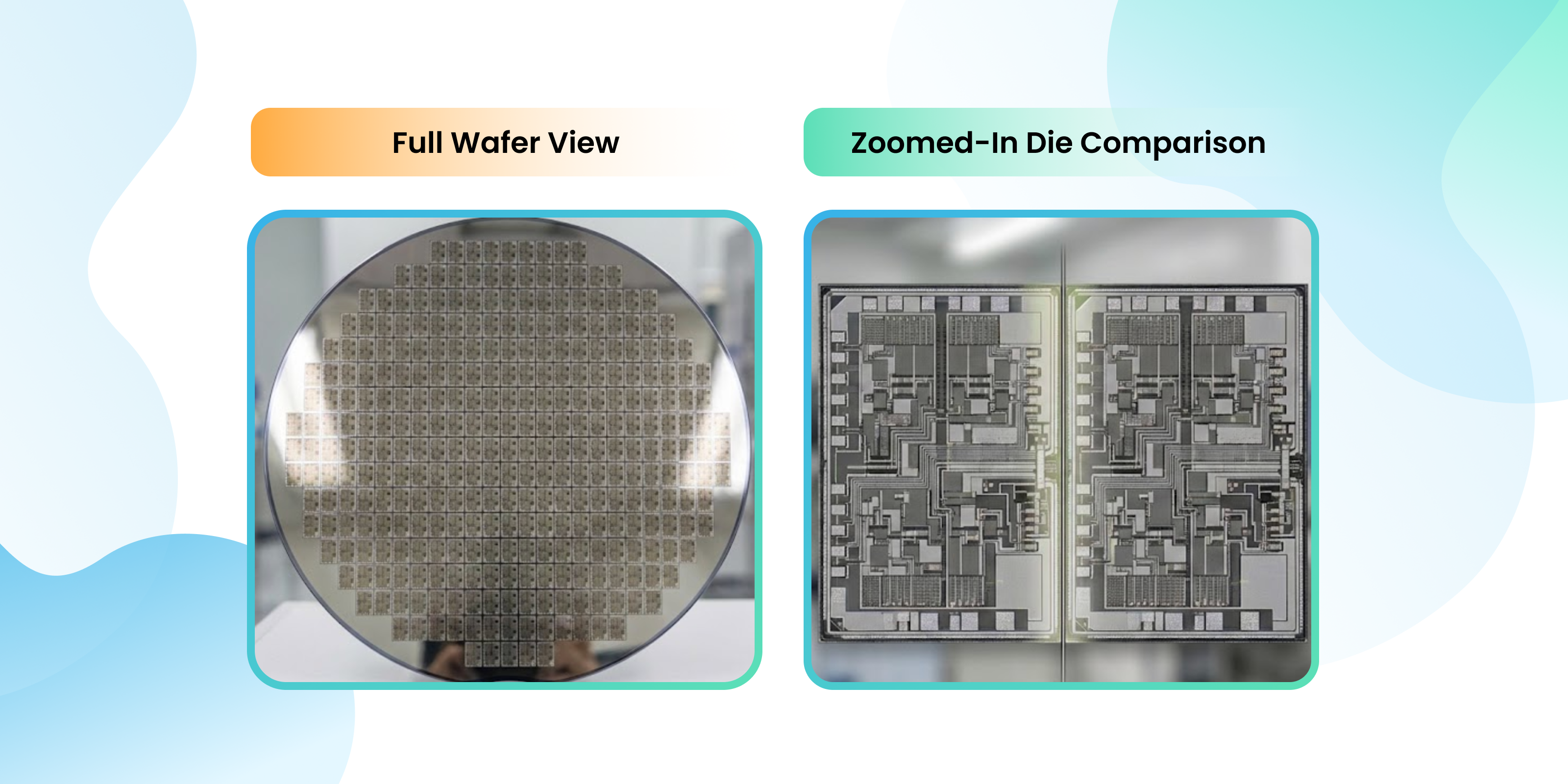
In the world of semiconductor manufacturing, we are currently racing toward Angstrom-level precision. We are building structures so small that a single stray dust particle looks like a mountain. To find these defects, fabs in this case used Scanning Electron Microscopes (SEM) to take high-resolution images of silicon wafers.
Die-to-Die Comparison
OEM Wafer inspection leverages the repetitive nature of silicon manufacturing through die-to-die comparison. By comparing images of nominally identical adjacent dies, the system can isolate process-induced defects—such as missing features or line distortions—while ignoring intended patterns. This transforms inspection into a precise change detection task, where any deviation between neighbors signals a potential manufacturing flaw. It is widely used today to detect yield impacting issues.
The catch is that OEM AOI tools are tuned conservatively. They prioritize not missing defects, which means they flag aggressively. The result is high overkill: a large fraction of AOI-flagged candidates are good dies that simply had minor imaging differences from their neighbour. To make AOI output usable downstream, fabs run a second classification layer, typically AI-based, whose job is exactly two things:
- Recover false positives coming out of AOI.
- Bin the true positives into defect classes (particle, scratch, pattern deformation, etc.).
This is the layer our work lives in.
2. The Problem Inside the 2nd Layer
The 2nd AI classification layer sees a flagged die image and has to decide: real defect, or AOI false alarm?
For most candidates, a well-trained classifier can make that decision from the flagged die alone. But a meaningful subset of genuinely defective dies carry defects that are indistinguishable from normal patterns when viewed in isolation. They are only recognisable when the flagged die is put side-by-side with a known-good adjacent die, exactly the die-to-die matching that AOI uses.
So the 2nd layer has a choice:
- Don't use die-to-die. The classifier misses these subtle defects and they escape into downstream production.
- Use die-to-die. The classifier catches them but now the 2nd layer inherits the same failure mode that plagued the OEM layer it was built to clean up after: every sub-pixel shift between the two dies gets read as a defect.
So the real challenge is to bring die-to-die comparison into the 2nd layer in a way that catches the escape-prone defects without reproducing the shift-induced false positives that made the OEM layer over-flag in the first place.
The rest of this article is about that.
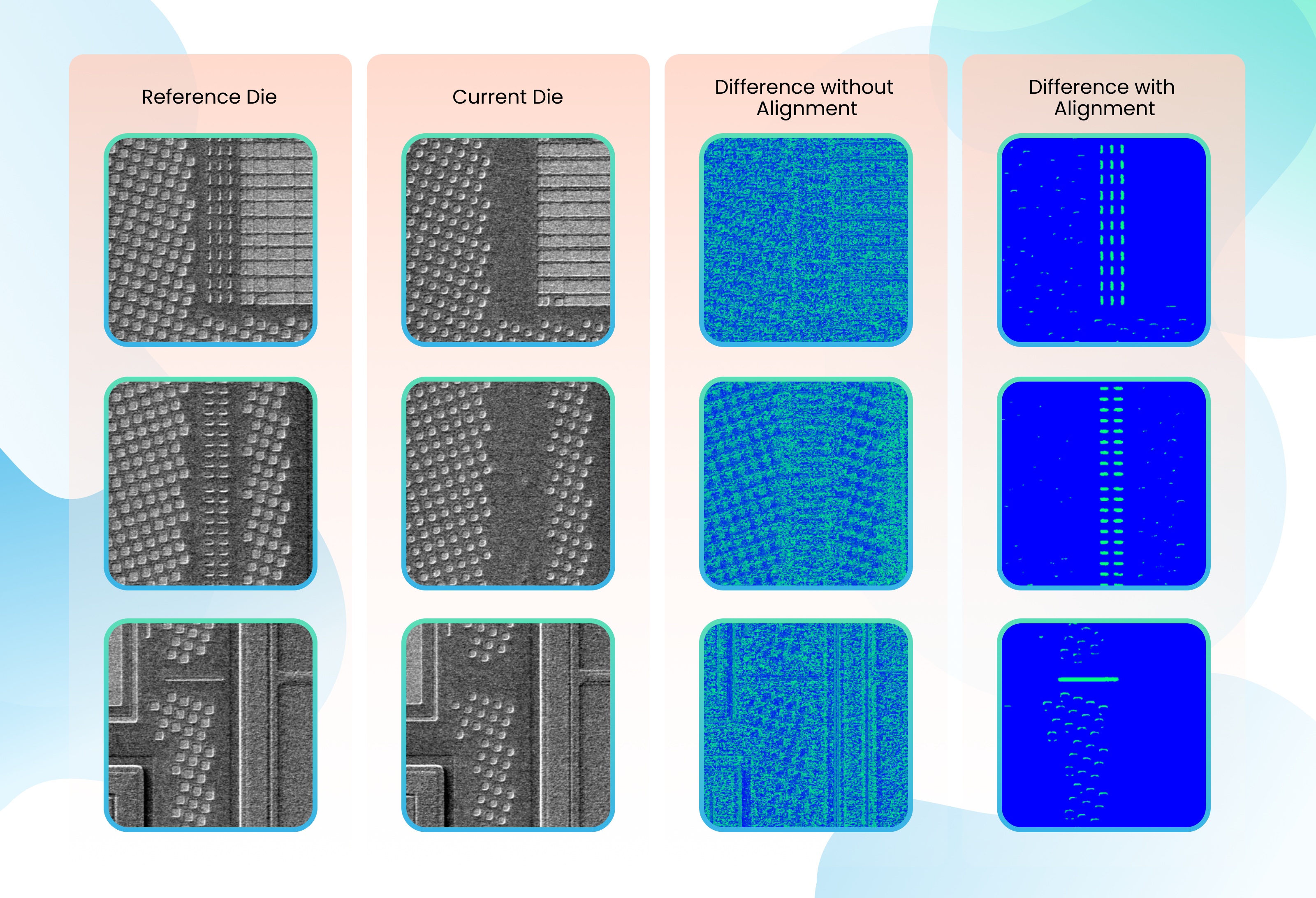
3. Understanding False Positives
When two "identical" adjacent dies are imaged and subtracted pixel-by-pixel, the resulting difference image should be nearly black except where a real defect exists. In practice it usually isn't, because:
- The wafer stage drifts slightly between the two captures.
- Optics can wobble sub-pixel amounts.
- Sampling grids between the two images don't land on the exact same coordinates.
Even a fraction of a pixel of shift causes every pattern edge to show up as a difference. This one failure mode of mild translation misalignment accounts for the bulk of the false positives die-to-die comparison generates.
That is the specific problem we solved.
4. Translation-Based Registration: The Core Model
In stable inspection setups:
- The imaging geometry is mechanically tight.
- Rotation and scale changes between adjacent dies are negligible.
- Translation (horizontal + vertical shift) dominates the misalignment.
This makes translation-based registration both sufficient and optimal, if it can be made fast enough. The model assumes the moving image is the same as the reference image, shifted in x and y, and estimates those shifts to sub-pixel accuracy so the two images line up before subtraction.
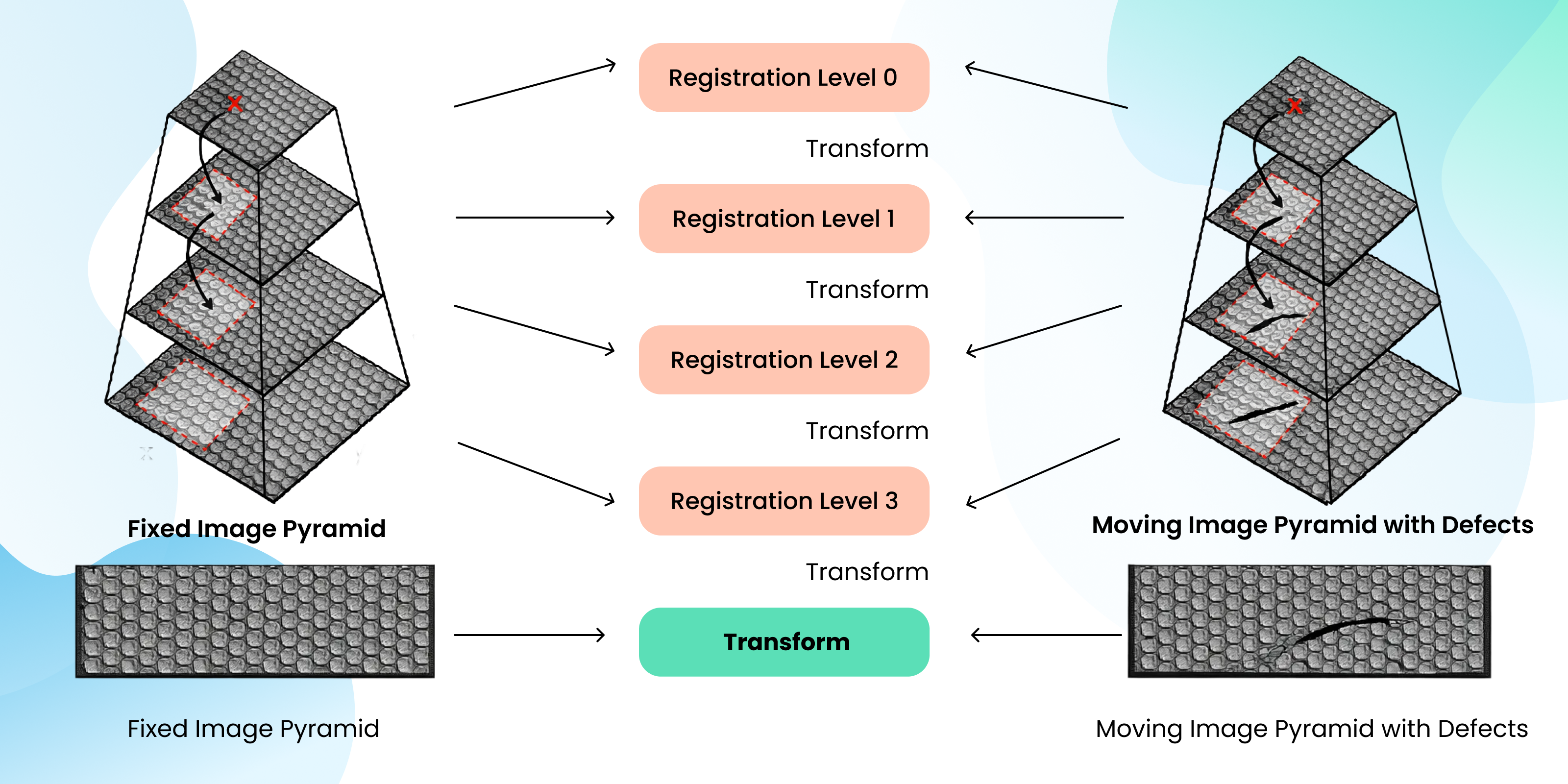
5. Pipeline: Start Blurry, Finish Sharp
The pipeline utilizes a pyramidal image registration approach to align fixed (reference) and moving (test) die images. The idea is simple: don't try to align two high-resolution images in one go. Start with blurry, low-resolution versions to find the rough position of shift, then gradually sharpen and refine.
We do this in three steps:
- Shrink both images into a stack of progressively smaller versions, blurry at the top, full resolution at the bottom.
- Align the smallest versions first. They're cheap to process and fine details don't distract the algorithm, so it quickly locks onto the big-picture shift.
- Pass that answer up to the next level and refine. Repeat until we're back at full resolution, where only a tiny sub-pixel correction remains.
Because each step starts almost-aligned, the math converges fast and doesn't get stuck on local pattern matches. The final result is a clean sub-pixel shift, so real defects stand out instead of getting lost in alignment noise.
6. Handling the Speed aspect
Aligning two die images is basically asking the computer to do the same small calculation: "how much did this pixel move?" for every single pixel in the image. For a 4K image, that's tens of millions of tiny calculations. The speed depends almost entirely on how many of these calculations the computer can do at the same time.
Traditional ways:
Think of the computer as a grocery store with only a few checkout lanes. Every pixel has to queue up, get scanned, and move on before the next one can be served. For a small image the queue clears quickly, but for a 4K image the line stretches out the door. A few specifics that make the traditional approach slow:
- The work is done pixel-by-pixel, or in small blocks, inside nested loops one after another.
- Each pixel's math isn't simple arithmetic; it involves heavy number-crunching (interpolation, gradients) that takes real time per pixel.
- Even with modern CPU tricks, only a handful of pixels can be processed at once.
- Double the image size and the work roughly quadruples so large, high-resolution dies hit the ceiling fast.
What we developed: thousands of lanes open at once
We rebuilt the same algorithm to run in a way that creates thousands of checkout lanes simultaneously. Since each pixel's calculation doesn't depend on its neighbours, we can hand every pixel its own lane and process the whole image in parallel instead of in sequence.
Concretely:
- Every pixel gets its own worker: interpolation, gradient, and comparison all happen at the same time.
- Thousands of cores chew through an entire image level in one go.
- Dedicated hardware handles the "peek between pixels" math (texture sampling / interpolation) almost for free, which used to be the slowest step.
- Every stage of the pipeline from shrinking images, applying shifts, computing differences, runs in this same parallel fashion.
As a result, we can register large die images orders of magnitude faster than traditional ways, enabling real-time or near-real-time inspection in high-throughput semiconductor manufacturing.
7. Performance Results
We benchmarked this release on high-resolution die images (0.5K–4K) and the findings were as follows:
- Baseline: ~300 ms per image pair.
- New implementation: ~5 ms per image pair.
- Speedup: ≈60× per pair.
At 5 ms per pair, registration is no longer the throughput ceiling of the 2nd classification layer. It means we can afford to run die-to-die comparisons on every candidate without slowing the layer down.
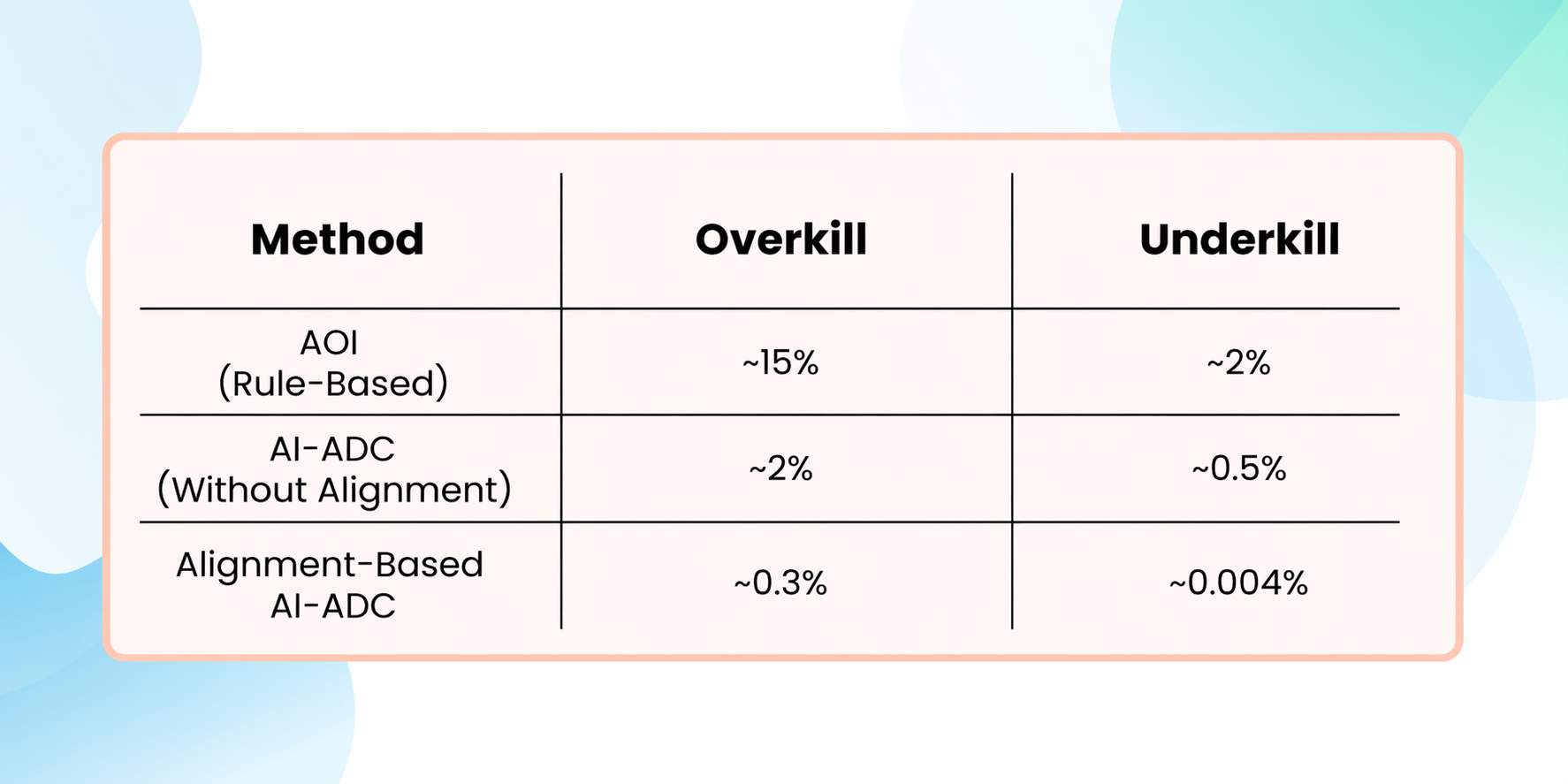
When we compare these approaches side by side, the impact of alignment becomes very clear. Traditional AOI methods tend to generate a high number of false alarms because they are sensitive to noise and small variations, while also missing subtle defects. Pure AI-based ADC improves defect detection, but without proper alignment, the model often gets confused by positional shifts, leading to unstable predictions and increased false positives. In contrast, combining fast, accurate die alignment with AI creates a much cleaner input for the model. This allows the system to focus on true process-induced differences rather than irrelevant shifts, resulting in both higher defect detection rates and significantly fewer false alarms. In practical terms, alignment is what transforms AI from “good” to “production-ready” in wafer inspection. Below is the comparison table :-
8. Impact on AI Model Training for Defect Detection
- Accurate and fast image registration has a direct and critical impact on AI model training for semiconductor defect detection. When die images are misaligned, pixel-level differences caused by registration errors appear similar to real defects. This introduces label noise into training datasets, confusing supervised learning models and reducing their ability to generalize.
- By using this approach, the resulting difference images contain only true physical variations, such as cracks, voids, or pattern deformations. This significantly improves the signal-to-noise ratio of the training data. As a result, vision models can learn defect-specific features only.
- It also enables large-scale dataset preparation, allowing thousands or millions of die image pairs to be aligned efficiently. This makes it feasible to continuously retrain AI models with fresh production data, adapt to process drift, and improve yield learning. In practice, faster and more accurate registration leads to cleaner training labels, faster convergence, and higher defect detection accuracy in AI-driven inspection systems.
9. Examples
Below are examples of the Results:
Defocus Defects
Missing Holes Defects
10. Conclusion
The 2nd classification layer exists to undo OEM overkill without letting defects escape. That mission is in conflict with itself the moment the layer needs die-to-die comparison to catch subtle defects.
Sub-pixel registration resolves that conflict. It lets the 2nd layer keep the detection benefits of die-to-die comparison while structurally eliminating its dominant false-positive mode. The 60× speedup is what makes this practical at ~5 ms per image, the 2nd layer can afford to align every candidate and treat die-to-die comparison as a routine tool rather than an expensive last resort.
Technical Glossary
Wafer
A circular slice of silicon on which semiconductor devices are manufactured. A single wafer can contain hundreds or thousands of identical chips.
Die (plural: Dies)
An individual chip patterned on a wafer. After manufacturing, each die may be cut out and packaged as a standalone chip.
Die-to-Die (D2D) Comparison
An inspection method where one die image is compared against another nearby die image. Because the dies are designed to be identical, any difference indicates a potential defect.
ADC (Automated Defect Classification)
A system that automatically analyzes inspection images to classify defects (e.g., particle, scratch, pattern deformation) without human intervention.
SEM (Scanning Electron Microscope)
An imaging tool that uses electrons instead of light to capture extremely high-resolution images of wafer features at nanometer or angstrom scale.
Image Registration (Alignment)
The process of aligning two images so that corresponding features overlap precisely. In wafer inspection, this ensures that differences between images reflect real defects, not camera or stage movement.
Translation-Based Registration
A form of image registration that corrects only horizontal and vertical shifts. It assumes no rotation or scaling, which is often valid in stable semiconductor inspection setups.
Sub-Pixel Accuracy
Alignment precision finer than one pixel. Required in semiconductor inspection because even tiny misalignments can create false defects.
Image Pyramid (Multi-Resolution Representation)
A set of progressively downsampled versions of an image. Coarse images capture large structures, while fine images preserve detailed features.
Similarity Metric
A numerical score that measures how well two images match after alignment. Higher similarity means better alignment.
NCC (Normalized Cross-Correlation)
A similarity metric that compares image patterns while being robust to brightness or contrast changes. Commonly used in inspection pipelines.
Interpolation
The process of estimating pixel values at non-integer positions when an image is shifted or warped.
Parallelism
Executing many computations at the same time. Image registration is highly parallel because many pixels and many candidate alignments can be evaluated independently..
Signal-to-Noise Ratio (SNR)
A measure of how much meaningful defect information is present compared to noise. Accurate alignment significantly improves SNR.
Yield
The percentage of functional dies on a wafer. Improving defect detection accuracy directly impacts yield and manufacturing cost.