

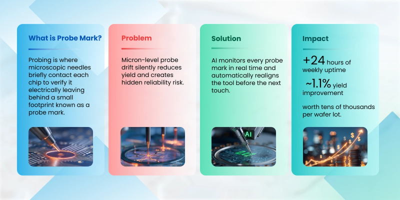
In the world of high-end electronics, we are building features so small that the physical world itself starts to work against us. Before the microchips inside our phone or car are even cut from their silicon sheets, they go through a critical testing stage called Wafer Sort. Here, a high-precision machine called a Prober uses microscopic needles to touch small metal contact points on each chip, known as Die Pads. When the probe touches a pad, it creates an electrical connection that allows the chip to be tested. These pads are tiny, only 30–50 microns wide, roughly half the width of a human hair.
Each time the probe lands on a pad, it leaves a tiny physical mark called a Probe Mark. In a perfect process, this mark lands in the center of the pad and causes no harm. But in real factories, nothing stays perfectly still. As the machine runs, the heat from its own motors causes metal parts to expand by a few microns, and the constant vibration from the floor causes the machine’s arm to slowly wander. We call this Machine Drift.
As the machine drifts, the probe mark moves toward the edge of the pad. If it touches the boundary, the chip is ruined immediately. More subtly, manufacturers define a safe area inside the pad called a Safety Zone. If the mark lands outside this zone, the chip may pass the test but still develop hidden weaknesses called latent defects. These defects don’t show up right away but they can appear later during packaging, assembly, or even after the product is in a customer’s hands.
At this microscopic scale, a tiny shift of just a few microns can affect thousands of chips before anyone notices. What seems like a small mechanical issue quietly becomes a major yield, reliability, and brand-risk problem.
In fact, a McKinsey study found that electrical testing alone contributed nearly $19 million in yield loss for one manufacturer, highlighting how tiny physical errors can lead to huge costs.
Taking the next leap forward in semiconductor yield improvement | McKinsey
We solved this by turning each probe mark into a feedback signal that allows the machine to measure its own drift and correct itself automatically. This closes the loop between observation and action, preventing silent yield loss and enabling continuous realignment as tolerances shrink.
By shifting from periodic manual checks to real-time self-correction, the system improves equipment uptime, stabilizes yield, and reduces the risk of hidden defects. What was once a slow, reactive process becomes continuous and predictable at production scale.
Solution: From Periodic Calibration to Continuous Control
Historically, fabs have managed this risk through periodic manual calibration, stopping tools, inspecting under microscopes, and making best-guess adjustments. While it was effective in the past, this approach struggles to keep pace with today’s advanced notes technology where devices are getting smaller and bond pads are shrinking.
We took a fundamentally different approach by closing the loop with AI illustrated in figure 1. Rather than using the prober’s camera as a passive observer, we turned it into an active sensor. After every probe touchdown, high-resolution images are analyzed by AI vision models that accurately determine where the probe mark lands relative to the pad’s safe operating zone. The system quantifies drift in real time, converts that insight from pixels into physical microns, and sends an immediate correction back to the tool, autonomously realigning the probe before the next die is tested.
This all happens in milliseconds, using standard factory interfaces, without slowing production.
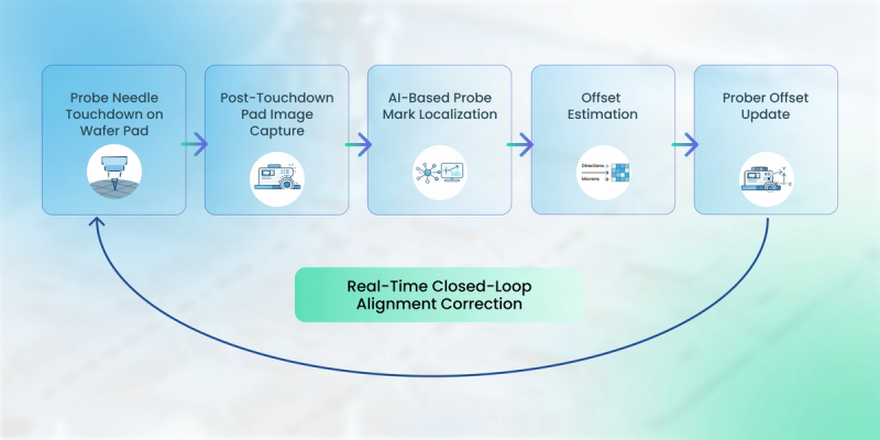
Figure 1
Here is the logic of how the data flows from a raw picture to a physical correction:
- The Input: Raw Vision
The moment the needle lifts, the system captures a high-resolution photo of the pad illustrated in figure 2. This raw image is fed into our AI vision model.
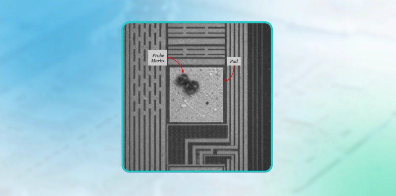
Figure 2
- The Processing: Recognizing the Shapes
The AI acts as an intelligent observer. It looks at the raw image and first recognizes the pad so it knows where the probe was supposed to land. It then finds the probe mark left by the needle. At the same time, it ignores anything that does not represent the actual touchdown, such as reflections from the metal surface, lighting variations, scratches, or small foreign particles. This allows the system to focus only on the true probe landing position and avoid being misled by visual noise.
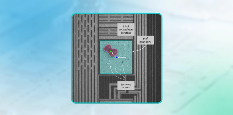
Figure 3
- The Logic: Measuring the Gap
The system calculates the displacement between the mark’s actual center and the ideal touchdown location. It identifies exactly how many digital pixels the machine has drifted, for example, "the probe mark is 8 pixels too far to the right." - The Transformation: Mapping Pixels to Reality
Digital pixels are translated into physical action by a second algorithm. Using known camera parameters, it maps those digital pixels into real-world 3D units. It knows exactly how many physical "microns" the machine needs to move to get back to the intended center. - The Output: Autonomous Realignment
The final correction is sent directly to the machine’s brain (the controller) using a universal language called SECS/GEM. Before the next chip is even touched, the machine has already realigned its arm. This happens in milliseconds, meaning the machine is constantly "aware" of its own error and fixing it in real-time.
Impact: Why This Matters at the Factory Level
The impact goes well beyond better inspection. Moving from manual checks to autonomous correction changes the economics of wafer test operations:
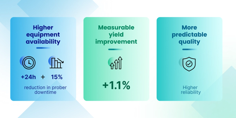
- Higher equipment availability: By eliminating frequent manual calibration stops, the tool remains in continuous operation instead of being taken offline every few hours. This shift alone recovered more than 24 hours of productive tool uptime per week, directly increasing throughput without adding equipment or headcount.
- Measurable yield improvement: Keeping probe contact consistently within safe zones improved yield by ~1.1%. At high volumes, that translates into significant dollar savings per lot.
- More predictable quality: By preventing marginal probe damage early, manufacturers reduce the risk of latent defects that escape tests but fail later during packaging or in the field.
As the industry moves toward advanced nodes, heterogeneous integration, and higher reliability requirements, control loops like these are becoming essential. The future of semiconductor manufacturing will be defined not just by better tools, but by smarter systems that can sense, decide, and correct in real time. This is where a true AI closed-loop system becomes essential, enabling manufacturers to not just see problems, but correct them automatically in real time and this is exactly where we are investing and executing.
“If AI can spot yield loss before humans see it, why are we still finding problems after the damage is done?”