

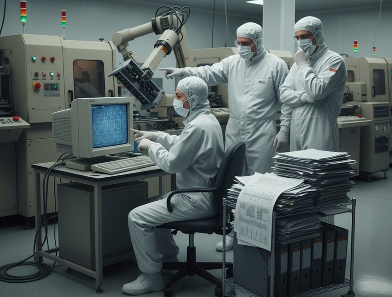
In today’s semiconductor factories, precision is everything. Robots move wafers seamlessly, tools work inside perfectly controlled environments, and every step of the process is tracked in real time.
And yet, despite all this sophistication, the biggest risk in semiconductor manufacturing today isn’t mechanical failure. It’s delayed decisions.’
A small defect or subtle process deviation can quickly turn into yield loss, wafer exposure, and weeks of root-cause analysis. Yet today, clues are scattered across YMS, DMS, FDC, SPC, and MES. Defects are tracked by counts or density. Process drift is monitored with statistical rules or limits. And RCA still depends heavily on manual effort.
The Hidden Problem: Too Much Data, Too Little Context
Semiconductor fabs are extremely data-rich environments.
Different systems exist to answer different questions:
- Are defects increasing?
- Is a tool behaving normally?
- Are process limits being violated?
- Where is each wafer in production?
But these systems were never designed to think together. Engineers are left doing the hardest job: Manually connecting information across time, tools, and process steps.
This leads to familiar problems:
- Alerts that trigger investigation but turn out to be false alarms
- Real issues that surface only after yield drops
- Engineers spending days correlating charts, logs, and images
- Root-cause analysis that takes weeks instead of hours
As fabs scale and complexity increases, engineering teams don’t scale at the same pace. The workload grows but human attention does not. This is where traditional approaches begin to fail.
Why Traditional Automation Isn’t Enough
Over the years, automation has made factories faster and more efficient.
Inspections happen quicker, sensors capture more data, and dashboards make it easier to monitor everything. Yet most systems still rely on fixed rules and preset alerts, which means problems can be missed or false alarms triggered.
These approaches work well for known problems. They struggle with new, subtle, or interacting issues.
Manufacturing today doesn’t just need automation. It needs understanding.
Turning Manufacturing Data Into Intelligence
This is the problem Sixsense.ai set out to solve.
The core idea is simple:Manufacturing data shouldn’t just be collected, it should be interpreted in context.
Instead of looking at defect data, tool data, and process data separately, Sixsense.ai connects them into a single intelligence layer that understands:
- Patterns across tools
- Changes over time
- Relationships between cause and effect
To do this, the platform brings together three tightly connected capabilities.
ClassifAI: Making Sense of Defects
Inspection tools generate enormous volumes of defect and wafer map images (SEM, optical, X-ray, etc.). Most machines are rule-based, producing high false positives (overkill) to prevent escapes. Operators manually review these results to safeguard yield
ClassifAI, a deep learning–based AI technology, automatically classifies millions of images across inspection tools (AMAT, KLA, Onto, Camtek, and more), cutting operator workload by 90%+ while reducing false alarms and escapes.
Production-ready models can be launched in <2 days directly by defect experts; no dependence on data science teams. Built on the latest deep learning architectures, ClassifAI enables fine-grained classification across hundreds of defect classes, with near-zero escapes and high yield recovery.
Multiple customers in advanced packaging have deployed models with 0% escape in production, across hundreds of devices, running with minimal maintenance using very few AI models.
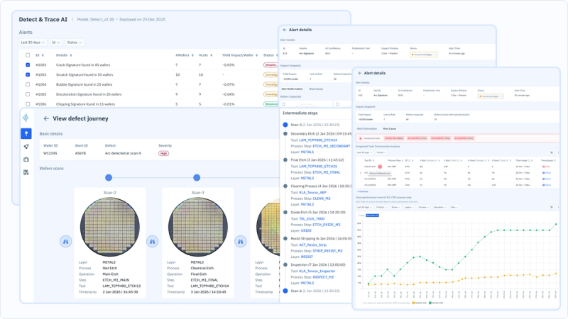
DetectAI: Catching Problems Earlier
DetectAI continuously monitors inspection, metrology, and tool data to detect early signs of systemic issues in wafers and lots. Its key goal: flag, as early as possible, when a lot should be held.
Examples include:
- Recurring wafer map signatures of a critical defect, even if not caught by SPC
- Overlapping deviations across multiple metrology parameters that signal yield impact
- Combinations of FDC parameters that eventually lead to metrology drift
DetectAI shifts manufacturing from reactive response to early intervention, helping teams act before yield is impacted.
TraceAI: Connecting the Dots to Root Cause
TraceAI analyzes a wafer’s entire processing history and data trail to surface the most likely process modules and tools responsible for the issue.
Today, engineers rely on JMP, Tableau, and Spotfire to identify the top suspect areas. TraceAI reduces the effort needed to collect and correlate siloed data, including defect images, wafer maps, metrology, and inline test data. It automatically gathers evidence, rules out possibilities, and narrows down root causes more quickly.
Even when only a few wafers are impacted, TraceAI leverages historical instances to ensure engineering knowledge and experience are preserved and reused. This reduces repetitive workload for yield teams by >50%.
What Changes When Decisions Get Faster
With ClassifAI, DetectAI, and TraceAI in place, fabs move from reactive problem-solving to proactive, knowledge-driven manufacturing:
Faster Decision-Making: Engineers spend less time gathering and cleaning data and more time acting on insights. Decisions on lot holds, process interventions, and yield recovery can happen hours or days earlier.
Reduced Scrap and Yield Loss: By catching defects and systemic issues earlier, fabs prevent unnecessary scrap, reduce escapes, and recover yield that would otherwise be lost.
Higher Engineer Productivity: Routine tasks such as manual defect review, cross-referencing data across tools, and hunting down root causes are automated, reducing repetitive workload by more than fifty percent.
Preserved and Scaled Knowledge: AI captures historical patterns, correlations, and engineering experience, making insights repeatable and reusable even as teams change or new devices are introduced.
Operational Consistency Across Fabs: Models can be deployed across multiple tools, products, and sites, creating standardized detection and analysis while minimizing the need for specialized AI expertise on every line.
The Bottom Line: AI transforms fabs from reactive problem solvers into predictive, intelligent, and self-learning operations, turning massive data into real-time action and laying the foundation for the autonomous factory of the future.